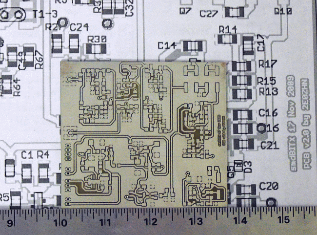
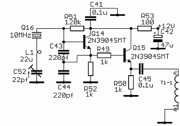
If you are looking for a different Bitx to build, this one's for you. It's based on the version 3 Bitx but using surface mount devices and a board designed by Elia, M0ZHN. The board shown below is one of his prototype boards. I assembled it and made some suggestions that were incorporated in his bitxsmd version 4. All files for the smd version 4 including pcb gerbers can be found at Bitx20 groups.io
This project is definitely not for the beginner! The small size of the surface mount devices require special techniques and equipment to assemble. The board will be assembled in individual stages and tested. When all stages are assembled and tested, the coupling capacitors will be installed combining the single stages into a fully functioning ssb exciter.
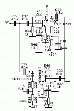
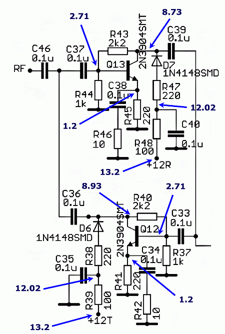
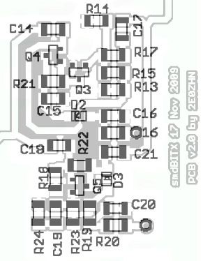
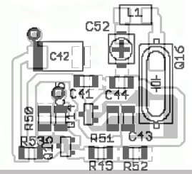
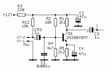
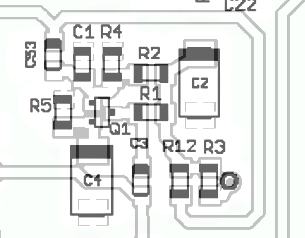
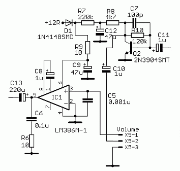
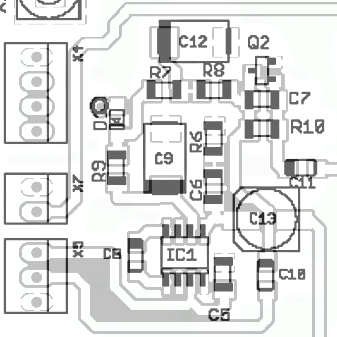
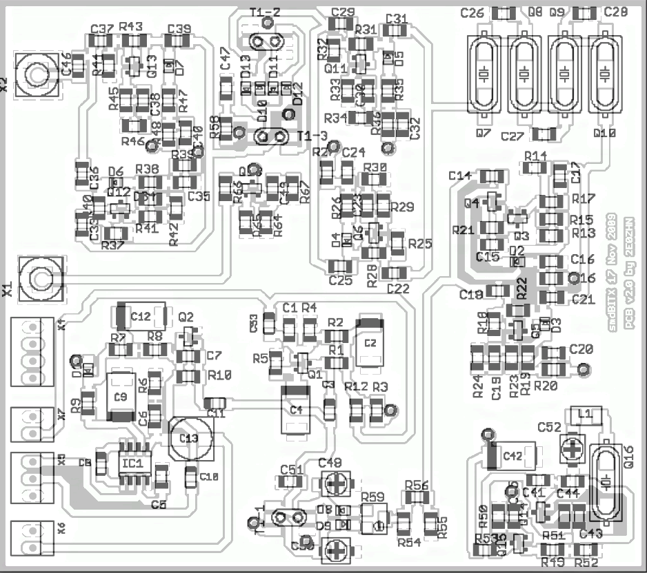
You can see the complete schematic at SMD Bitx schematic and the complete board layout at X-ray component placement
Many of the stages will be modeled using LTspice. It is a free simulation software available from LTspice The section files will be listed in each section.
The stages can be assembled in almost any order but we will start at the rf input/output.
Install header pins for X4, X5, X6, and X7. This will allow you to power the board using a standard Version 3 power supply.
I've added 3 LTspice simulations for the RF amplifier. The only difference between these is the Spice command telling the software what to do. The schematics are all the same. After starting LTspice, click on the link to download the file and then run it by clicking on the "running man".
DC operating point - Mouse over and point and it tells you the dc voltage at that point. Look in the lower left corner of your display.
Frequency Response - Draws a gain vs frequency plot of the waveform at your selected point. Move the probe to the spot you want to see plotted. Normally the output signal.
Transient Analysis - Provides an oscilloscope view of your selected point. Be sure to take a look at View FFT to see the spectrum analysis of the selected point.
 \
\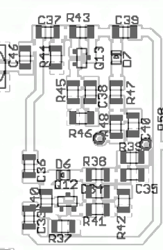
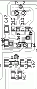
Install the following components on the board using the drawings above for position.
|
RF Amplifier Components |
||||
| Designator |
Quantity
|
Value |
Description
|
|
|
R42,
R46
|
2
|
10 ohm
|
resistors | |
|
R39, R48
|
2
|
100 ohm
|
resistors | |
|
R38,R41,R45,R47 |
4
|
220 ohm
|
resistors | |
|
R37, R44
|
2
|
1k
|
resistors | |
|
R40, R43
|
2
|
2.2k
|
resistors | |
|
C33, C34, C35, C36, C37, C38, C39, C40,
C46
|
9
|
.1uf
|
capacitors | |
|
D6, D7
|
2
|
1N4148
|
diodes | |
|
Q12, Q13
|
2
|
2N3904
|
transistor | |
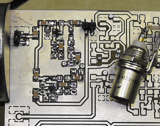
After assembly, the board should look like this. The connector is a standard BNC.
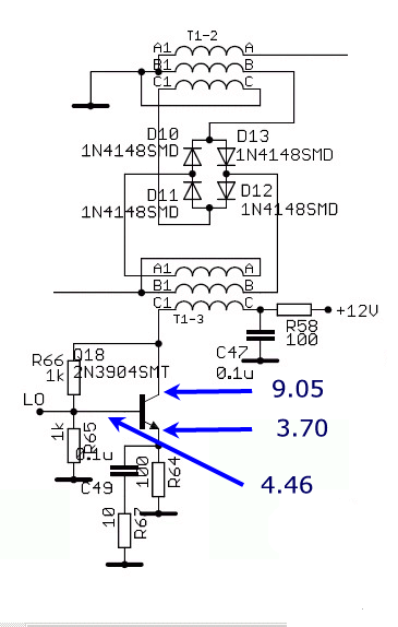
Compare your voltages to the voltages below. To measure the receiver side, apply voltage to the R side . To measure the transmit side, apply the voltage to the T side. Do not apply voltage to both simultaneously.
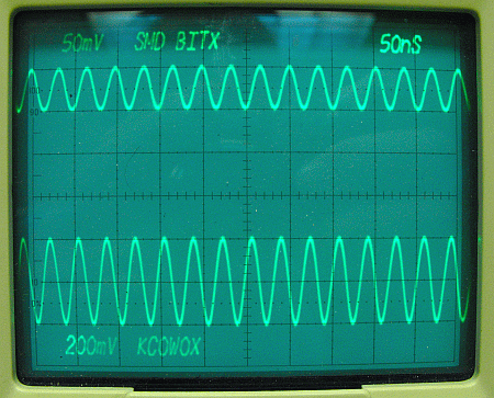
Now for a test. If you ran the LTspice simulation, you found that it predicted about 21.7 db of gain at 1MHz and at 30MHz, it dropped to 20.3 db. Lets see what it actually does.
First we have to setup the network analyzer.
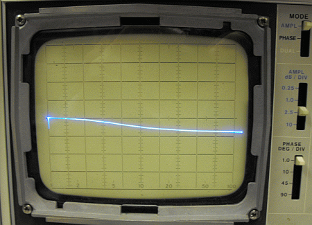
Here we are displaying the test port plotted against the reference port from 1MHz to 50Mhz. Normally it should be a flat line from one side to the other as all that is being tested is basically the cabling. I have to do some special setup and that is causing the loss.The only thing that is particularly important here is the loss at 30 MHz. 30 MHz is 6 divisions from the left as each division is 5MHz. The db/div is set at 2.5db so at 30MHz, we are down about 1.75db.
Lets hook the amp in the circuit.
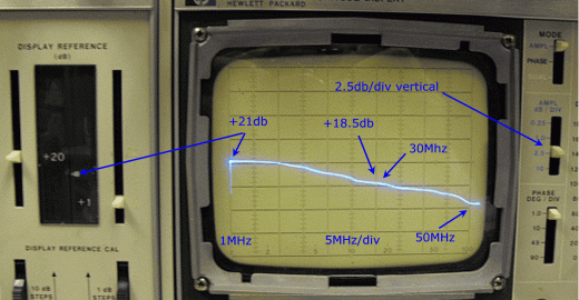
The display reference setting now says the center line vertically is +21db. The display is a hair above the center line so we are pretty close to the predicted +21.7 db of gain. Lets look at 30MHz. That's 6 divisions to the right. It's down about .9 divisions so .9 x 2.5db is 2.25db. Remember we were down -1.75 db with our original setup so we need to subtract that out. 2.25 - 1.75 = 0.5db. The simulation predicted 21.7 - 20.3 = 1.5db. Our measurement isn't perfect but there is a lot of room for error to creep in due to screen interpolation and component values. I can live with my measured results.
Lets make the same measurements by using a signal generator and a scope at 1MHz and 30MHz, measure the output, and using db=20log (eout/ein), calculate the gain.
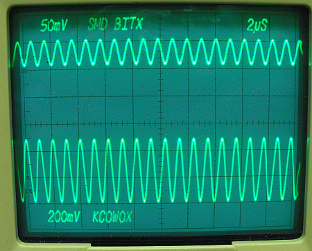
First 1MHz.
db=20log(500/50) = 20db. Close to our 21db simulation.
Now 30MHz.
db=20log(400/50) = 18.06. Still pretty close to the simulation. If you get different values, probably lower, make sure you are using a 10x scope probe. The 120pfd or so loading of a x1 probe really changes things at 30MHz. A x10 probe has around 12pfd's of capacitive loading.
The end result of the test is this amplifier will work for any of the HF bands. We'll retest it later with a load after completing the mixer stage.
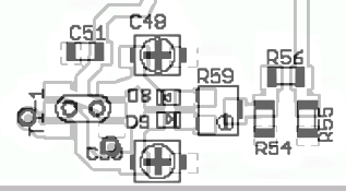
The link to the LTspice file is Mixer LTspice file There are 2 added components on the schematic. R1 represents the input resistance of the following circuit. Try changing it and plotting the result. The other is C1 coming from the local oscillator. It exists in the RF amplifier circuit. We need to add it here to keep from affecting the base bias of Q18.
|
Mixer Components |
||||
| Designator |
Quantity
|
Value
|
Description
|
|
|
R58, R64
|
2
|
100 ohm
|
resistor | |
|
R65, R66
|
2
|
1k ohm
|
resistor | |
|
R67 |
1
|
10 ohm
|
resistor | |
|
C47, C49
|
2
|
.1uf
|
capacitors | |
|
D10, D11, D12, D13
|
4
|
1N4148
|
diodes | |
|
Q18
|
1
|
2N3904
|
transistor
|
|
|
T1-2, T1-3
|
2
|
torroidal transformer | ||
|
Q18
|
1
|
2N3904
|
transistor | |
|
1st IF Components |
||||
| Designator |
Quantity |
Value |
Description |
|
|
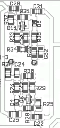
R27. R36 |
2 |
100 ohm |
resistors | |
|
R25, R32 |
2 |
1k ohm |
resistors | |
|
R30, R34 |
2 |
10 ohm |
resistors | |
R26, R29, R33, R35 |
4 |
220 ohm |
resistors | |
|
C25, C29 |
2 |
.1uf |
capacitors | |
C22, C31 |
2 |
100pfd | capacitors | |
|
D4, D5 |
2 |
1N4148 |
diodes | |
|
Q6, Q11 |
2 |
2N3904 |
transistor |
|
|
Crystal Filter Components |
||||
| Designator |
Quantity |
Value |
Description |
|
|
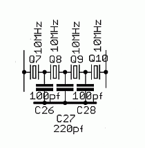
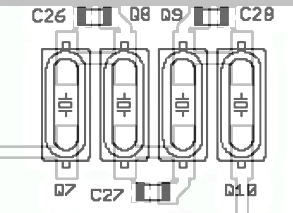
C26, C28 |
2 |
100pfd |
capacitors | |
|
C27 |
1 |
220pfd |
capacitor | |
|
Q7, Q8, Q9, Q10 |
4 |
10 MHz |
crystals | |
|
2nd IF Components |
||||
| Designator |
Quantity |
Value |
Description |
|
|
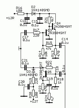
R16, R20 |
2 |
100 ohm |
resistors | |
|
R18 |
1 |
1k ohm |
resistor | |
|
R24 |
1 |
4.7 ohm |
resistor | |
R17, R19 |
2 |
220 ohm |
resistors | |
R13, R23 |
2 |
470 ohm |
resistors |
|
R21 |
1 |
4.7k |
resistor |
|
R15 |
1 |
47k | resistor | |
R22 |
1 |
2.2k | resistor | |
R14 |
1 |
10k | resistor | |
|
C14, C15, C16, C18, C19, C20 |
6 |
.1uf |
capacitors | |
C17, C21 |
2 |
100pfd | capacitors | |
|
D2, D3 |
2 |
1N4148 |
diodes | |
|
Q3, Q4, Q5 |
3 |
2N3904 |
transistor |
|