Below are some of the easy-to-check waveforms for a bitx20a VFO. The voltages displayed may be slightly lower than yours as this bitx board has had the 9.1 volt zener replaced with the 78L08 voltage regulator modification which lowers the VFO voltage from 9.1 volts to 8 volts.
The oscilloscope volts/division can be read in the upper-left portion of the picture. The sweep speed time/division is displayed in the lower-right side of the display.
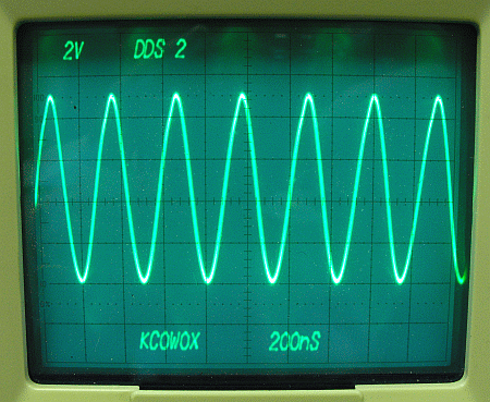
First, we will look at the oscillator, Q8 base. An easy place to check is the DDS #2 pad.
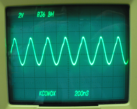
The Q8 emitter signal can be seen at the buttonhook of R36.
The signal fed to Q7, the oscillator buffer, is at the buttonhook of R32. This is the R32-C90 junction. Q7's job is to provide a constant high impedance load to the oscillator, Q8 and a low impedance drive signal to Q6.
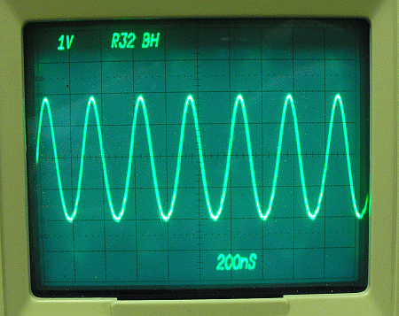
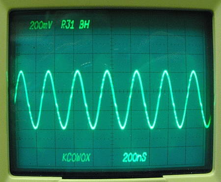
Q7 emitter checkpoint is the buttonhook of R31.
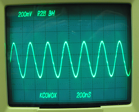
Q6 base signal checkpoint is the buttonhook of R28. This should be the same signal as Q7 emitter.
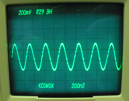
Q6 emitter checkpoint is the buttonhook of R29.
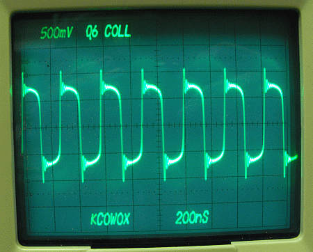
Q6 Collector.
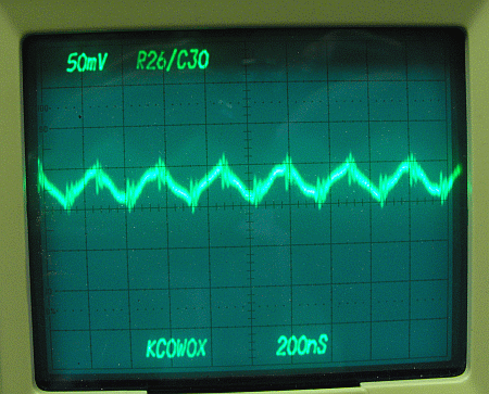
R26 - C30 junction. This should be a very small signal as C30 is coupling the signal to ground to keep it out of the power supply line.